General
|
General Information |
The 4040 is an enhanced follow-on processor to the Intel 4004. The 4040 was used primarily in games, test, development, and control equipment. The package of the 4040 is more than twice as wide as the 4004 and has 24 pins vs. the 16 of the 4004. The 4040 added 14 instructions, larger stack (8 level), 8K program space, 8 more registers, and interrupt abilities (including shadows of the first 8 registers). The 4040 family is also referred to as the MCS-40. |
|
Production |
4 Qtr, 1974 |
| Designers | Ted Hoff, Federico Faggin, Stan Mazor, Masatoshi Shima |
Architecture
| Type | Data Word | Address Space | Clock | Instruct- ions | Assists | Reg’s GP | Reg’s Math | Reg’s Index | IO Ports | Stack | Interrupts | Memory |
| PMOS,CPU | 4-bit | 8Kb program,5Kb data | 740kHz,2 Phase | 60 | BCD | 0 | 1 | 24 4-bit | NA | 8×12 | NA | NA |
Packages
|
Chip Name |
Package |
On-Chip Identification |
Picture |
General Comments |
|
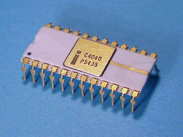
C4040 |
White/Gold CerDIP, 24-pin |
C4040 |
 |
|
|
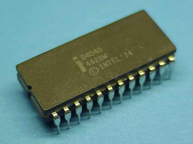
D4040 |
Gray Ceramic, 24-pin DIP |
D4040 |
 |
|
|
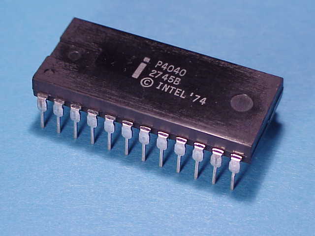
P4040 |
Black Resin, 24-pin DIP |
P4040 |
 |
Related Chips
|
Related Chips |
Intel 4004 |
|
Second Sources |
None |
| Support Chips | MCS-4 Chips4001 (ROM), 4002-1 (RAM), 4002-2 (RAM), 4003 (Shift)4008 (EPROM Interface), 4009 (EPROM Interface)
MCS-40 Chips 4201 (Clock, Avail 1Q/75), 4207 (I/O), 4209 (I/O), 4211 (I/O), 4265, 4269, 4289 (System Memory Interface), 4308 (1K ROM)
Supplemental Chips 4702 (EEPROM), (4316 2K ROM), 4101 (128K RAM), 3216/3226 (4-bit Bus Driver) |